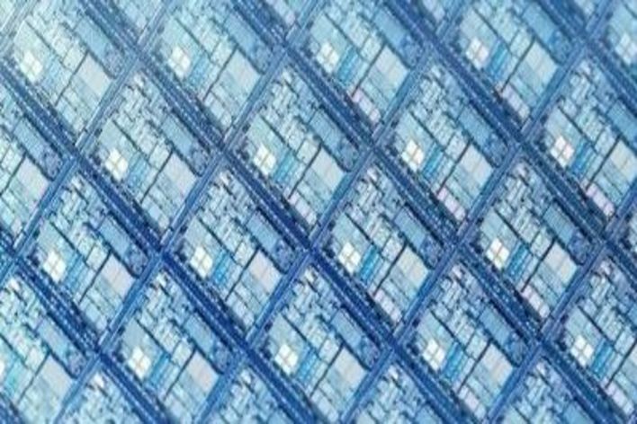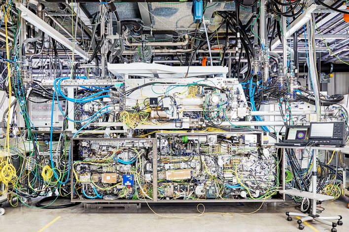
What does the world’s largest industrial laser from TRUMPF have to do with the way we will communicate in the future? Quite a bit, as it turns out. The latest generation of computer chips would not exist without this giant laser, and nor would state-of-the-art smartphones. But first things first: It takes highly complex lithography equipment to produce the latest generation of microchips. Netherlands-based ASML is the only company that manufactures these systems, which work with EUV light. And TRUMPF’s colossal laser is the only device that can generate this EUV light. Weighing more than 10 metric tons, it consists of 450,000 individual parts. As the system’s light source, this laser generates plasma with a temperature of 220,000°C, which is 30 to 40 times hotter than temperatures on the surface of the sun. The giant laser is aimed at a stream of tin droplets inside the lithography system, where it strikes and flattens 50,000 of these tiny droplets every second. Actually, the giant laser takes two shots at each of these tin droplets, with the second hit transforming the flattened droplet into plasma that emits the precious EUV light. Of course, the laser’s light beam has to shaped in a very specific way to strike 50,000 individual droplets per second. The laser shoots compressed light packets at the tin droplets, which is why experts call it a pulsed laser. Each of the 50,000 pulses per second consists of a small, compact group of light particles, hurled at the droplets in a tight bunch. To hit their target properly, they have to arrive at precisely the right instant, not a moment too soon or too late; otherwise, the impact will not flatten the tin droplet. In the worst-case scenario, the second laser shot misses its mark so that the attempt to generate EUV light fails. And that brings us to Michael Kösters.
Kösters and his team lend shape to light
Video: Michael Kösters zu seiner Nominierung zum Deutschen Zukunftspreis
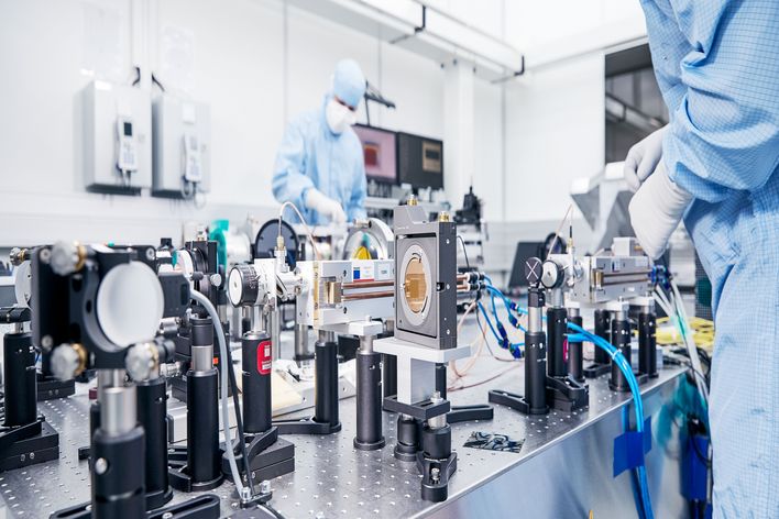
Michael Kösters and his team developed the High Power Seed Module. One of the key components for generating EUV, it has helped make this technology commercially viable around the world. The High Power Seed Module ensures the light particles hit each tin droplet nearly simultaneously in a compact bunch, which gives form to the light beam. Normally, some light particles in the laser pulse lead the pack while others lag behind. This module provides the means to shape this laser pulse and control how each of the 50,000 droplets per second is bombarded. With the benefit of this module, ASML’s huge EUV systems will be able to produce the world’s most powerful microchips for many years to come. “We have increased the EUV yield by a factor of two. We would have remained at well below 125 exposed wafers per hour without the High Power Seed Module. And that would have made the use of this technology commercially unfeasible,” says Kösters.
Not content to merely plant this seed, the entire TRUMPF development team continues to refine the system. They are now designing, testing and building new prototypes. “We and our partners ASML and Zeiss have arrived at 175 wafers per hour with the Seed Isolation Module. This has helped EUV technology to its breakthrough – and it is already enabling the reliable production of the latest generation of microchips for smartphones. The brightest future for this technology is yet to come, for example, in connected cars and in artificial intelligence,” says Kösters.
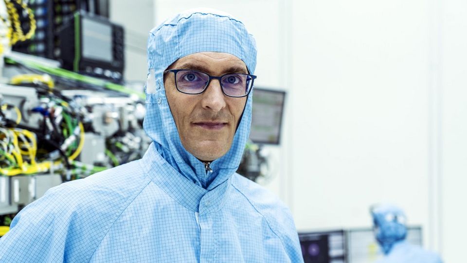
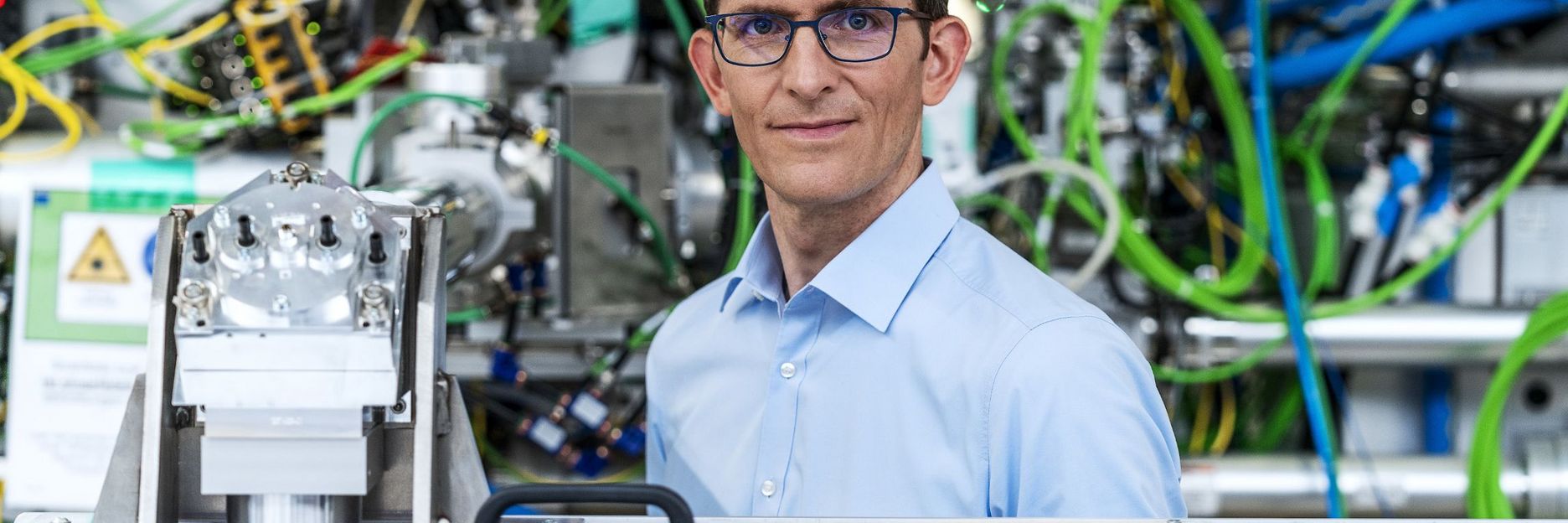
Michael Kösters has dedicated his career to developing the world’s most powerful pulsed industrial laser. He and his team helped EUV lithography to a breakthrough with the High Power Seed Module.
© DZP / Ansgar Pudenz
Development of EUV technology - a collective effort of thousands
What fascinates Michael Kösters most about his work is the technical complexity of the EUV system. “I am particularly impressed by the speed at which we innovated in this project. We are a relatively young team, so the atmosphere is much like that of a startup.” He also likes the collaboration with colleagues at TRUMPF, ZEISS, ASML and many hundreds of other partners in industry and research, such as Fraunhofer IOF. “Thousands of colleagues were and are involved in the development of EUV technology, without whom this success would never have been possible. In this respect, my team and I are really only representatives of a tremendous collective effort,” says Kösters.
Michael Kösters joined TRUMPF in August 2010. He joined the EUV project in spring 2011, where his work would have a major impact. TRUMPF sent him inter alia to the Netherlands for four months to coordinate services with ASML, a partner in the EUV project. Before joining TRUMPF, the 40-year-old physicist who holds a doctorate was a research fellow at the University of Bonn’s Institute of Physics. During this time, he worked on optical crystals of the type used in small laser pointers and wrote a dissertation entitled, “Optical cleaning of lithium niobate crystals.” In his free time, Kösters goes jogging, rides his road and mountain bikes, and hikes a great deal.