Generation of EUV radiation using a CO2 high-power laser system and tin
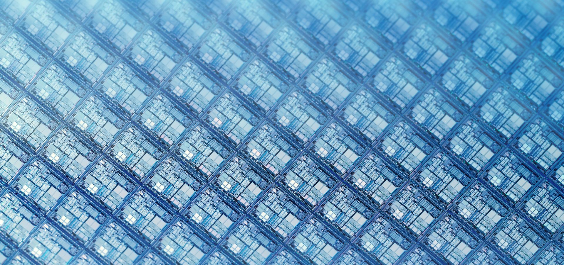
Be it mobile end devices, autonomous driving, or artificial intelligence – miniaturization and automation in our digital world are placing ever-increasing demands on computer performance. The result: more and more transistors need to be placed on the semi-conductors inside chipsets. This is not a new phenomenon, as even one of the Intel founders knew that the number of transistors in an integrated circuit doubled around every 18 months. This has been dubbed "Moore's Law" and still applies today; in fact it is how integration densities of up to 100 million transistors to one square millimeter have been reached. The size of semi-conductor structures is inching closer and closer to atomic dimensions. High-performance laser amplifiers by TRUMPF play a central role in the production of these chips. They help to create a luminous plasma which delivers extreme ultraviolet radiation (EUV) exposure to the substrate. In close cooperation with ASML, the world's largest manufacturer of lithography systems, as well as Zeiss, the optical systems manufacturer, TRUMPF has developed a one-of-a-kind CO2 laser system which can process over 100 substrates an hour.
From tin droplets to substrate exposure: the EUV lithography process
Modern computer chips generally come in nanometer dimensions and can only be produced by complex exposure processes with the help of lasers. This is where the conventional approach with UV laser exposure by excimer lasers increasingly reaches its limit. Smaller structural sizes in ranges of less than ten nanometers can no longer be created with this existing method. These delicate structures require exposure to even shorter wavelengths - rays in the extreme ultraviolet (EUV) range.
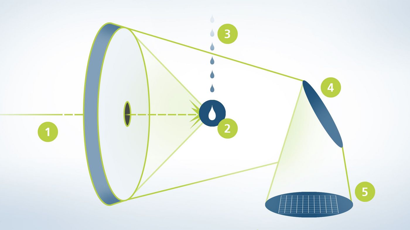
The major challenge of EUV lithography is to generate radiation with the optimal wavelength of 13.5 nanometers. The solution: A luminous plasma generated by laser radiation that delivers this extremely short-wave radiation. But how is the plasma initially produced? A generator drops tin droplets into a vacuum chamber (3), then a pulsed high-power laser (1) by TRUMPF impacts the passing tin droplets (2) – 50,000 times per second. The tin atoms are ionized, and an intensive plasma is created. A collector mirror captures the EUV radiation emitted by the plasma in all directions, bundles it, and finally transfers it to the lithography system (4) for exposure of the wafer (5).
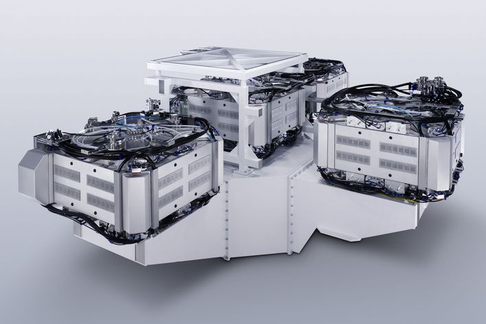
The laser pulse for plasma radiation is delivered by a CO2 laser system with pulse capabilities that was developed by TRUMPF – the TRUMPF Laser Amplifier. The high-power laser system is based on CO2 continuous wave laser technology in a power range of over ten kilowatts. It amplifies a CO2 laser pulse of just a few watts of average power more than 10,000 times in five amplifier stages, creating tens of kilowatts of average pulse power. The peak pulse power reaches multiple megawatts. TRUMPF components are part of the lithography process from laser beam creation, amplification to their direction to the tin droplets. The combination of a complex technical matter that constantly brings about unique and new solutions, very fast series introduction cycles, and the implementation of specific customer requests creates an exciting field for developers, service engineers, and production workers.
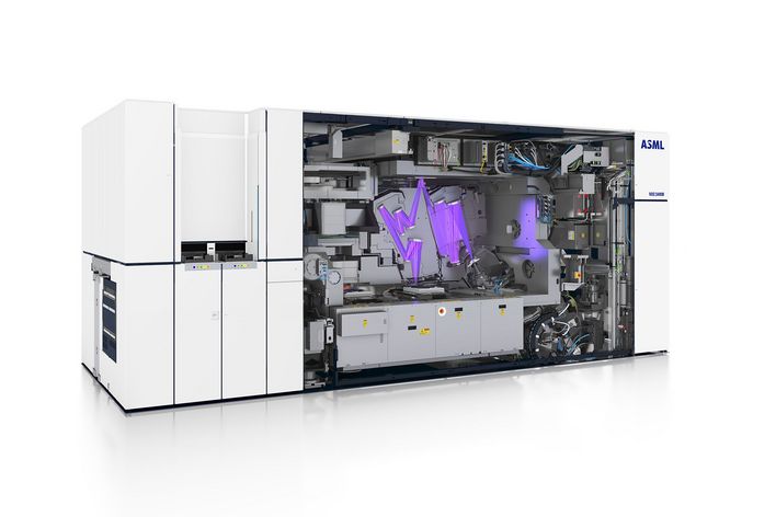
TRUMPF has developed an internationally unique CO2 laser system in close cooperation with renowned partners. ASML, the largest manufacturer of lithography systems in the world, served as integrator and delivered the components for droplet creation and the scanner. The EUV optics were by Zeiss. These components make it possible to process more than 100 substrates an hour – enough for series production. This makes EUV lithography not only a technical, but also a complete commercial success for chip manufacturers worldwide.


