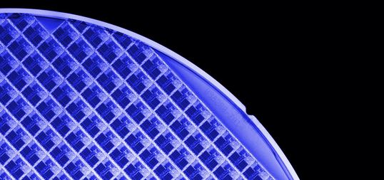
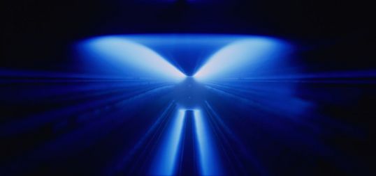
Material removal is used to make electronic component structures from thin layers. Conductor paths or transistors, for example, can then be created. Ionizing the molecules of an assist gas produces ions, which are accelerated in the plasma's electric field towards the substrate surface.
Reactive ion etching enables directional selective ablation, a requirement for the production of microelectronic components and MEMS (micro electro-mechannical systems). To precisely control ion flow and energy, different generators with different excitation frequencies are used to generate bias voltages.


