It all starts with an inconspicuous raw material: silicon. It is melted from quartz sand in huge furnaces to form cylindrical crystals. These are then cut into wafer-thin wafers. At 30 cm in diameter, each wafer is about the size of a family pizza and later forms the basis for hundreds to thousands of chips.
The special thing about silicon is that the raw material has both conductive and insulating properties. Silicon can therefore sometimes conduct electricity and sometimes not – depending on how it is processed. This is exactly what makes silicon a so-called "semiconductor".
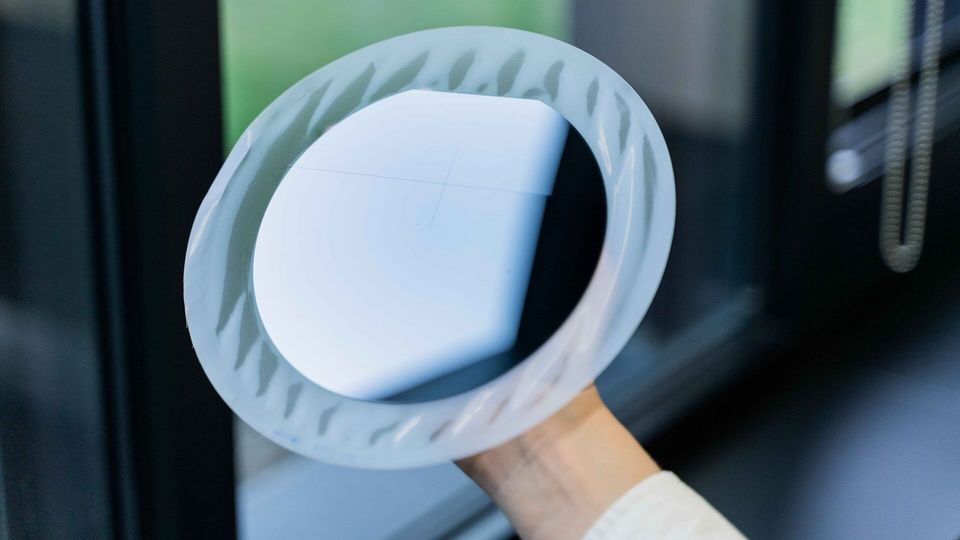
The wafer: At first it is nothing more than a shiny disk, but it becomes hundreds to thousands of chips.
Layer-by-layer to the brain of modern electronics
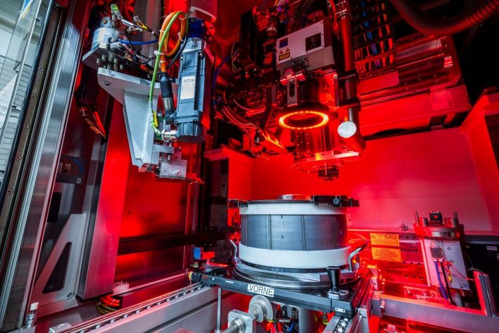
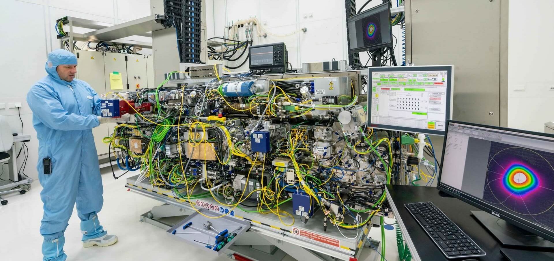
Now the high-tech work begins. A conductive or insulating layer is first applied to the wafer in a plasma chamber. Generators from TRUMPF supply precisely controlled energy. They keep the voltage, frequency and current intensity exactly within the range required by the processes.
The wafer is then coated with a light-sensitive lacquer. This prepares it for the heart of chip production: lithography. High-energy, extreme ultraviolet (EUV) light draws tiny patterns in the paint through targeted laser exposure. TRUMPF plays a key role here worldwide, as the high-power laser is one of the central components of this technology when it comes to the most powerful microchips.
The exposed areas are then etched away in a plasma process to create the finest conductor paths in the material. Here too, TRUMPF generators play an important role in controlling these complex etching processes.
Generators from TRUMPF tame the current and set the amperage, voltage and frequency to a highly precise value.
The heart of chip production: a component of the world's most powerful pulsed industrial laser, which is used to generate light to enable EUV lithography.

Extreme ultraviolet (EUV) light draws the subsequent conductor paths as tiny patterns in the light-sensitive coating.
Precision work in the nano range
This is followed by "doping", in which atoms of a material (typically boron or phosphorus) are introduced into certain areas of the resulting microchip. Here too, TRUMPF generators ensure the necessary accuracy in the process. The individual atoms change the electrical conductivity of the silicon. This makes it possible to conduct or block current flow in a targeted manner. This step lays the foundation for the digital logic of computers: 0 or 1 – block current or allow current to flow.
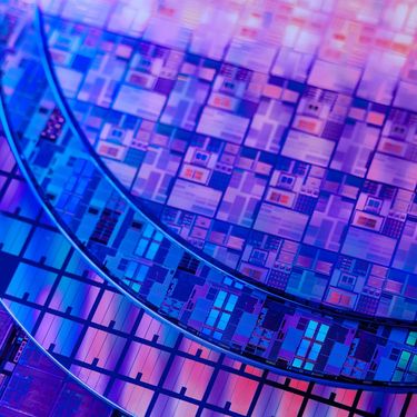
When the first layer is finished, the surface of the wafer is smoothed in a chemical-mechanical polishing process until it is mirror-like again. Then the process starts all over again: applying the layer, exposing, etching, smoothing – dozens of times in succession. In this way, interconnected structures grow that are millions of times smaller than a grain of sand.
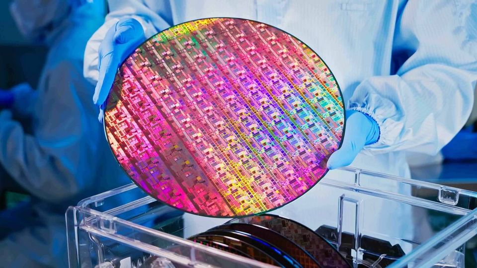
Up to thousands of individual chips are produced from one wafer.
In between, measuring systems regularly check the quality – with lasers utilized here too. Initially during production, later under load and temperature in the test. This is important because even the smallest errors can render entire batches with millions of chips unusable.
Once the last layer is complete, a laser cuts the wafer into hundreds to thousands of pieces. These are installed individually on printed circuit boards and in protective housings. The laser helps by exposing contact points, welding wires or marking serial numbers, for example. After final testing, the tiny components end up as finished microchips in smartphones, cars or medical devices.
No AI without TRUMPF. Our laser and plasma solutions are the backbone of modern semiconductor manufacturing. From EUV lithography to advanced packaging: Our technologies are used wherever the future is being created. Whether coating, exposing or etching – anyone who wants innovation and progress cannot ignore TRUMPF. We think ahead: Our solutions not only enable peak performance, but also resource-saving processes. Together with leading technology partners, we develop innovations that transform entire industries.