The most important laser applications in semi-conductor manufacturing
Discover our infographic, which vividly illustrates the key role of laser technologies in semi-conductor manufacturing, from the silicon crystal to the finished microchip. In the front end, laser processes can accompany the cutting, exposure, etching, doping and smoothing of the wafers, while precise laser measurements can ensure quality. In the back end, lasers can be used for separating, connecting, structuring and marking the chips. The illustration clearly shows how chip manufacturers can use lasers in numerous processes: As a tool for maximum precision, efficiency and quality.
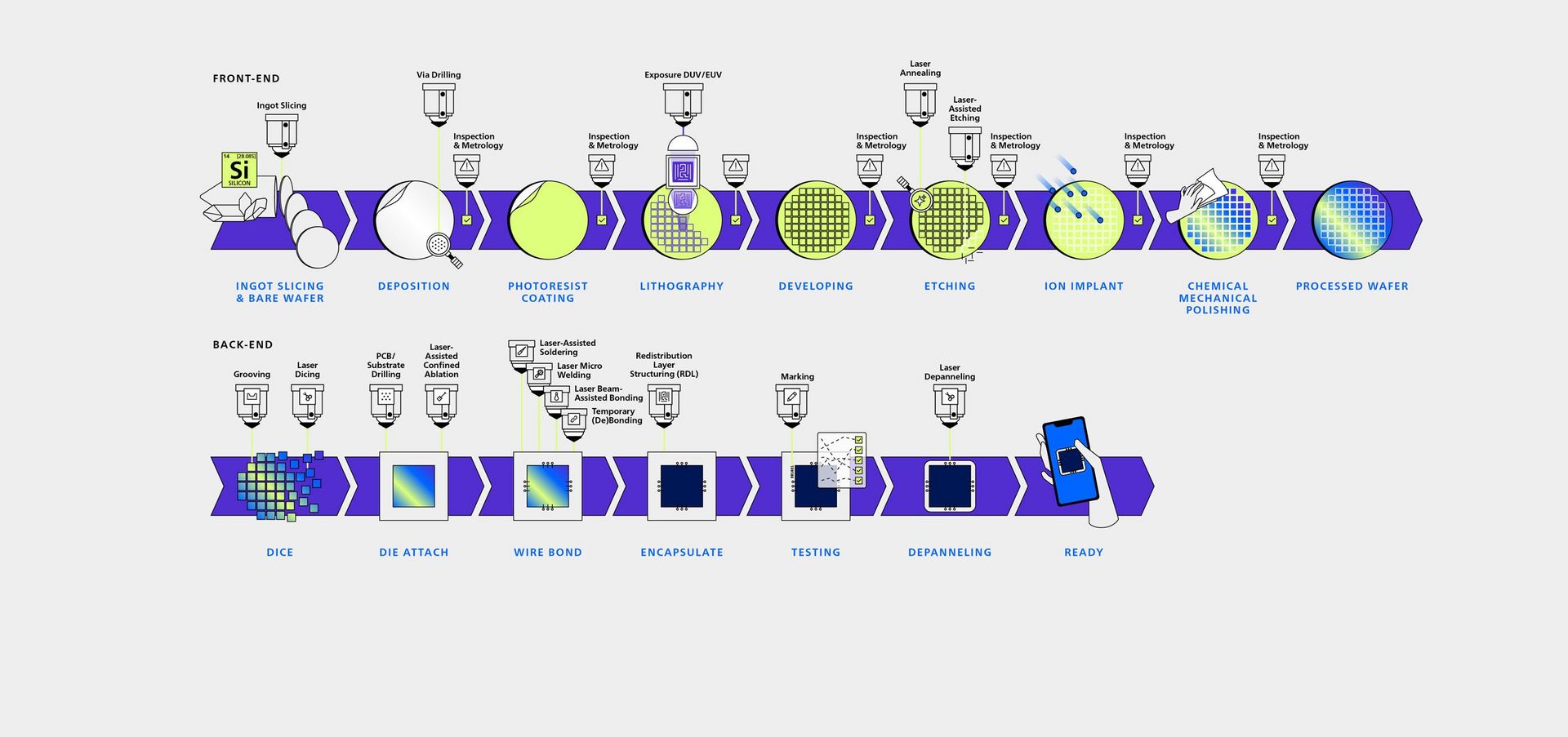
1. Ingot slicing
A laser cuts the silicon single crystal into extremely thin wafers in a way that is gentle on the materials.
2. Via drilling
Laser beams drill tiny vias into insulating and semi-conductor layers. They enable, for example, vertical connections between circuit layers in 3D chips.
3. Exposure DUV/EUV
Lasers are needed to provide deep ultraviolet (DUV) or extreme ultraviolet (EUV) radiation for the exposure process.
4. Laser annealing
The laser selectively heats near-surface areas of the wafer for a few nanoseconds. This heals crystal defects and activates dopants.
5. Laser-assisted etching
The laser heats specific areas to accelerate local etching. This is particularly helpful with complex shapes.
6. Inspection & metrology
Non-contact laser measurement and defect detection ensures quality and process control after almost every work step in the foundry.
7. Grooving
The laser cuts fine grooves into wafer or substrate material. This reduces the mechanical stress during subsequent dicing and increases the yield.
8. Laser dicing
A laser beam cuts the wafer into individual chips (dies) without leaving any particles. Laser processes are used particularly often for very thin wafers.
9. PCB/substrate drilling
Lasers drill tiny holes in printed circuit boards and substrates for electrical connections, especially in high-density assemblies.
10. Laser-assisted confined ablation
The laser selectively removes surface material, for example to expose hard-to-reach contact points.
11. Laser-assisted soldering
The laser heats tiny solder joints, thus connecting the chip and the substrate.
12. Laser micro welding
Laser beams melt fine wires at specific points, thus welding the contact points together.
13. Laser beam-assisted bonding
The laser prepares the thermocompressive joining of chip and substrate or housing by targeted heat input.
14. Temporary (de)bonding
The laser supports the necessary temporary bonding or debonding of chips and substrates during processing.
15. Redistribution layer structuring (RDL)
The laser structures the thin metal layer (redistribution layer) that carries signals from the chip to the outside and connects several chips together.
16. Marking
Marking lasers apply serial numbers, Data Matrix Codes or logos to the chip and housing.
17. Laser depanneling
The laser beam separates individual chips, modules or printed circuit board components from a larger assembly (panel).