Barely eight years ago, a family of four living in an industrialized country might have had two computers: a PC and a laptop. That’s still the case, but on top of this they now also own four smartphones — one for each family member — and a tablet PC that’s shared by everyone. Among the presents tucked beneath this year’s Christmas tree might even be the first smart watches, too.
To say that the electronic devices industry is in full swing is an understatement. People love their smartphones. They want more of them, and they’re always looking to buy a newer one. Nearly three million smartphones were sold every single day in 2013, or just over one billion units in total. In 2009 that figure was around 173 million — that’s growth of 480 percent in four years. And according to market researchers at IDC, 1.8 billion smartphones will be sold annually four years from now.
While there wasn’t even a market for tablet PCs our years ago, manufacturers sold 160 million of them in 2013.
Unlike the PC industry, the developing smart devices industry is still in its unruly infancy. In the shortest time, we’ve seen seemingly unassailable industry giants yield supremacy to newcomers. But even they cannot afford to rest on their laurels, as serious new manufacturers are already fighting their way into the market — more than ten from China alone — all looking to grab a slice of the pie.
Anyone wanting to take part in this competition requires two things: the ability to constantly bring out new features, and manufacturing processes that are ever more efficient and less expensive. These days lasers are already a key driver of innovation, for the latter in particular.
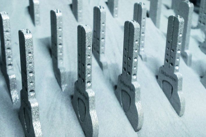
Cutting sapphire for smartphone camera protection
For instance, the industry is relying more and more heavily on materials for which laser processing is pretty much the only viable option. Materials such as sapphire, the word’s second-hardest substance, are ideal for use in devices that travel from hand to pocket several times a day, scraping against keys in the process. Transparent sapphire covers protect sensitive smartphone cameras from this kind of wear and tear.
But the durability of the material is both a blessing and a curse. Mechanical processing and polishing methods can be used in the watch industry, where batches are generally no more than a thousand units, but are simply unaffordable on the scale of production required by cell phone manufacturers — which is why these companies use lasers instead. With ultra-short pulses and the highest possible pulse peak intensity, lasers can cut sapphire quickly, accurately, without the need for reworking and, thanks to the most recent development, even with a stepped edge. Light is the only tool that has the potential to process the several hundred thousand units needed. Per day, that is.
Cutting and making contact of flexible film circuits
At the same time, lasers are increasingly finding their way into the interior of smart devices, too. Manufacturers have been calculating the available installation space in terms of cubic millimeters for quite some time now, playing “Tetris” with the electronic components to fit them in.
One of the ways they are able to do this is by using flexible film circuits made of polyimide, which can match the available space. This means that they can be cut to the exact size and shape required — to connect different functional groups, for instance. Lasers are perfect for this task, as they permit free forms, do not suffer wear and tear, manufacture with one hundred percent reproducibility, and exert no mechanical strain on the workpiece.
This trend is set to increase. Smart glasses, wristbands, watches — maybe even contact lenses — none can be made without irregularly shaped film circuit boards. Many printed circuit boards no longer have much in common with real-world boards. Most are thin films of three, four, five or more conductive and non-conductive layers. Many thousands of tiny, conductor-filled holes connect the conductive tracks in the various layers. And increasingly, these holes are being drilled using infrared picosecond lasers, which can punch thousands of holes per second while making contact with the conductive tracks (no thicker than a human hair) with an accuracy of within ten micrometers.

Display und Touchfolie: Ultrakurzpulslaser schneiden die
extrem dünnen und harten Displaygläser abrasiv. In einem neuen Verfahren
bringen sie intrinsische Spannung direkt ins Glas ein, damit es kontrolliert
reißt. Die beschichtete Touchfolie wird per Piko- oder Femtosekundenlaser
effizient und prozesssicher zugeschnitten. Und Infrarot- Laserlicht
strukturiert die leitenden Schichten auf dem Touchsubstrat.
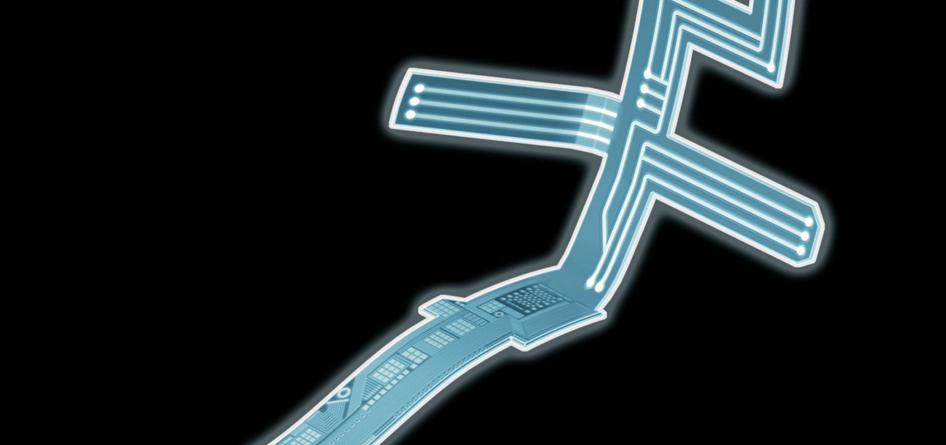
Folienleiterplatte: Laserlicht schneidet die flexiblen Folienleiterplatten in die richtige Form. Pikosekundenpulse bohren die Löcher, mit denen die Leiterbahnen übereinanderliegender Ebenen kontaktiert werden.
Saphir-Kameraabdeckung: Ultrakurze Pulse schneiden extrem harte Saphirplättchen, die als Schutz für die Smartphone-Kamera dienen. Seit Neuestem auch einbauoptimiert mit gestufter Schnittkante.
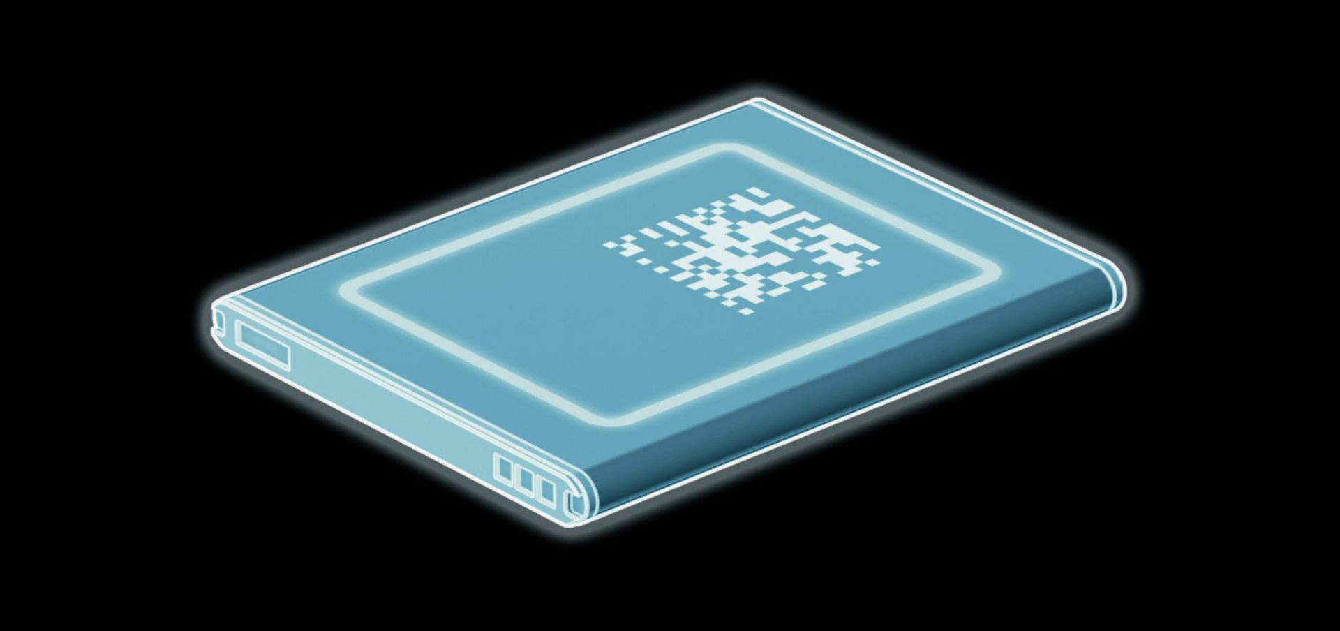
Akku: Gepulste Laser schweißen die Akkus, die danach per Markierlaser beschriftet werden: mit Firmenlogos, Datamatrix oder Seriennummern.
Gehäuse: Faserlaser schneiden die Konturen an Metallgehäusen, für ein hübsches Logo sorgt der Markierlaser. Für die Gehäuse der Zukunft aus Keramik, Titan oder Carbonfaser kommt bei den geforderten Stückzahlen nur Laserlicht als Bearbeitungswerkzeug infrage.
Machining display glass by laser
By far the most expensive component is the touch screen. The display assembly alone accounts for about a quarter of total production costs, making it the ideal place to look for expense savings. A display is made up of two glass sheets, each around 300 micrometers thick. Between them lie the transistors for controlling the pixels, the liquid crystals in the LCDs or the OLEDs, and one or two coated films for the touch screen functions.
The glass used is constantly being made thinner and tougher, which makes it even harder to process. It’s almost impossible to cleanly score and break this new glass. Etching is one viable alternative, but dry processes using lasers are always going to be less trouble.
Accordingly, new production lines increasingly feature ultra-short pulse lasers. They cut the glass in a cold process that does not cause thermal or mechanical stresses in the workpiece. As an added bonus, the lasers produce smooth edges that have no microfissures and require no reworking. This considerably reduces the likelihood of glass breakage.
Material modification inside the screen glass by ultra-short pulsed lasers
Very soon, however, we could see a much faster and more elegant process taking over the job. Instead of chomping its way through the material, pulse by pulse, in this method the ultra-short pulses modify an extremely narrow area inside the glass along the “cutting” line. The change creates an intrinsic tension that causes the glass to break cleanly and exactly, to within a hundredth of a millimeter, along this fault line. The first machines able to cut glass in this way have already been built.
Not only does this new cutting technique give manufacturers the opportunity to dispense with expensive intermediate steps in today’s industrial display screen manufacturing processes. It also allows the process to be reorganized. Because the laser cuts hardened glass quickly and without touch-up work, the future could see processing steps such as hardening, coating and structuring being carried out at a greater scale, on large panels. Lasers could then cut the large panel into smaller sections at the very end of the process.

Smart watches are another intelligent companion.
Picture: Fotolia
Flexible screens with OLED
Lasers are also the way forward for the screens of the future. Flexible OLED screens are the stuff of dreams for product de-signers and production engineers. Mounting organic light-emitting diodes on plastic films means that displays can be shaped, curved and flexible.
At the same time, flexible displays would make roll-to-roll manufacturing techniques a real possibility. They would simply be wound off and on, passing through various printing and coating machines as part of continuous processes before, for example, being cut into displays of all sizes by a laser beam in a final step.
OLED screens currently start life as a thin, liquid polyimide layer on a glass substrate. The polyimide hardens and forms the base film. Silicone layers are then applied for the transistors, onto which the actual OLEDs are then applied as screen pixels. To keep costs down, the silicone is applied in an amorphous layer and melted using a UV laser. During solidification the silicon crystallizes, which increases its conductivity and allows the transistors to switch faster, creating smoother images.
Solid-stat lasers for annealing
The process is called excimer laser annealing. However, the excimer laser gas resonators that give the process its name are very prone to malfunctions, meaning that production engineers have to spend hours every day maintaining and recalibrating them. For a long time there was no alternative, but now there is. Today’s reliable, high-power, solid-state lasers provide enough energy for this processing technique, even after the frequency tripling required to reach the UV spectrum.
Increasingly, lasers are being used to make the OLEDs themselves — at least indirectly. Display manufacturers produce OLED pixels using metal templates that are a little larger than a sheet of letter paper but just 30 microns thick and exhibiting a series of regularly arranged, tiny holes. The OLEDs are plotted through these holes as pixels 30 square micrometers in size. Because the extremely fine holes clog quickly, the metal template soon wears out and has to be replaced.
Clean solution for metal templates
Templates are usually made via a chemical etching process, but this has the drawback of creating holes with uneven edges, since the chemical’s concentration changes as material is etched away. The etching fluid uses itself up, so to speak. In contrast, ultra-short pulse lasers offer a far more precise and absolutely reproducible solution.
Not only is this pioneering method able to drill vertical, sharp edges in the metal template; it is also faster and cleaner. The extremely short pulses drill up to 200,000 holes in a single second, and there’s no need for chemicals.
After the coating process, the OLEDs have to be detached from the supporting glass substrate. The aim is, after all, to create a flexible display. There is yet another laser process that can help with this, called laser lift-off. Here a nanosecond UV laser beam is fired at the polyimide layer of the display from the back, through the glass. It heats the layer precisely where it touches the substrate, causing it to lose adhesion and peel off. And there you have it — the OLED display is finished.
Ultra-short pulse lasers cut display glass by abrasion or introduce intrinsic tension directly into it to insure that it breaks in a controlled fashion. They drill holes into flexible film circuits and cut sapphire panels, destined to cover and protect smartphone cameras. For cutting, structuring, ablation or drilling, in microproduction technology, lasers are being used more and more frequently.
Marking lasers mark QR codes or serial numbers on components of smartphones – the battery for example. They also apply an attractive logo on smartphone cases.
Due to their high beam quality, fiber lasers are your first choice for precision applications. For example they shape metal cases for smartphones and soon cases made of ceramics, titanium or carbon fibre.
Fiber-guided pulse lasers have been welding and cutting a wide variety of products and workpieces for decades, they also weld batteries for smartphones for example.
Using conventional processes, the high-tech electronics industry has come to accept rejection rates of 25 percent. Lasers, however, can achieve yields of 98 percent for all of the above applications — representing huge leverage for anyone looking to save on production costs.
The smartphone market is booming, with new electronics factories springing up in every corner of the Asia-Pacific region. Phones and tablets are soon to be joined by a wave of portable, flexible, high-tech computers designed to be worn as clothing or accessories: smart watches, smart glasses, smart whatevers.
These products could not exist without lasers, and lasers are driving their production forward. It’s just not possible to make tomorrow’s world using yesterday’s tools.
This article was first published in autumn 2014.