What is advanced packaging?
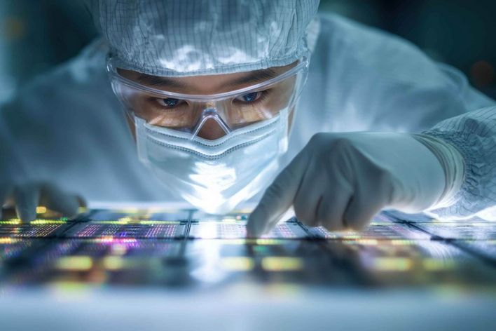
In what is known as advanced packaging, several chips with different functions are integrated to form an entire high-performance system. Depending on the design, they are arranged side by side or stacked on top of one another. This makes it possible, for example, to combine computing power, memory and other functions within a very small space. Extremely fine electrical connections ensure that the individual chips can exchange data quickly and efficiently. At the same time, the heat generated must be reliably dissipated. This makes advanced packaging much more than just a new design. The technology enables greater performance and higher energy efficiency in a smaller space, taking microchips to the next level of performance.
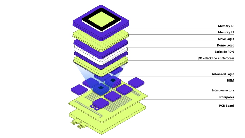
Multiple layers, different functions – in advanced packaging, specialised chip components for computing power, memory, and other functions are integrated into an entire, space-saving system.
Where is advanced packaging used?
Advanced packaging is becoming increasingly important in any application where a high level of computing power is required in a small space. One example is AI accelerators – specialised chips that process artificial intelligence tasks extremely quickly, such as training large language models or analysing massive amounts of data in data centres. To do this, processors, memory, and other chip components must exchange data extremely quickly. Advanced packaging shortens these pathways and makes systems more powerful and efficient. This technology also plays an important role in high-performance computing (HPC). This refers to high-performance computers used for particularly complex calculations, such as in research, simulation, weather modelling, medicine, or industrial development. In addition, there are applications in smartphones, smartwatches, vehicles, and networked factories. The demand for compact, fast, and energy-efficient chips is on the rise everywhere.
Why is advanced packaging so challenging?
Modern chip packages consist of millions of tiny structures, thin layers, delicate materials, and minuscule contact points. Even slight deviations can impair functionality. In mass production, every process must run consistently and reproducibly and ensure a high yield, because every deviation costs a fortune. This is where specialist technology partners come into play. TRUMPF is known to many as a laser specialist in metalworking and as a machine manufacturer. However, TRUMPF has long been supplying technology for the various steps in the semiconductor manufacturing process that make such modern chip packages possible in the first place.
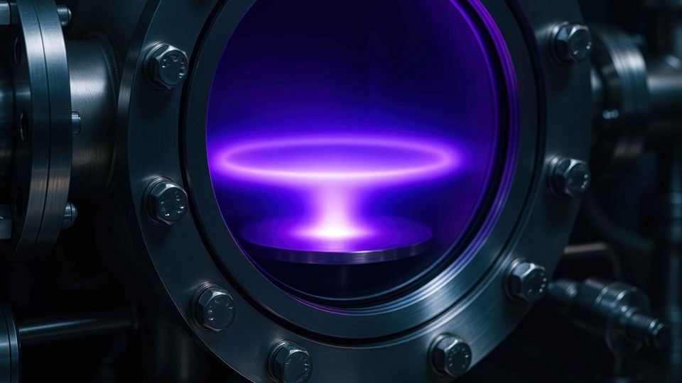
Plasma plays an important role in semiconductor manufacturing. It makes it possible to produce extremely fine structures and to selectively deposit or remove wafer-thin layers of material.
What role does plasma play in advanced packaging?
Plasma is an electrically excited gas. In semiconductor manufacturing, it removes material in a controlled manner, or builds up layers. In advanced packaging, plasma helps create fine interconnect structures and contact areas through which signals will subsequently flow between the chip components. TRUMPF plasma generators precisely control the necessary processes on wafers and substrates. This makes it possible to create uniform structures, build up layers in a controlled manner, and establish reliable electrical connections.
Where does the laser really come into its own in advanced packaging?
Lasers process materials non-contact and with precision. They cut, drill, structure, mark, apply localised heat, or assist with ablation and joining. This is important because new material types such as glass, thin wafers, dense substrates, and fine interconnect layers are essential in advanced packaging. One example where the laser really excels is in the production of vias – tiny through-holes that are later filled with metal using our plasma generators. This is how electrical contacts are formed between the layers in the chip package. TRUMPF's ultrashort pulse lasers precisely create such vias in substrates or intermediate carriers. Lasers also excel at structuring circuit traces and separating chips and packages. They operate locally, quickly, and without subjecting the material to thermal or mechanical stress.
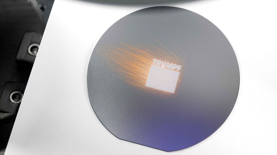
TRUMPF lasers process sensitive materials non-contact and with high precision. This opens up new possibilities for semiconductor manufacturing.
What materials are suitable for use as chip substrates?
One example of the next stage of development in advanced packaging is through-glass vias – fine holes that connect through glass. Until now, manufacturers have often used silicon for this kind of intermediate carrier. Glass can be used as an alternative in certain applications. It has favourable thermal properties, can be manufactured to be very flat, and can be processed into rectangular rather than round shapes. This helps save material and increase yield. The challenge lies in the processing. High-precision laser technology makes it possible to drill very fine holes in glass – quickly, with precision, and to a high quality standard. Materials used for cooling are also coming into focus. Silicon carbide could be a promising material for microfluidic cooling channels because it dissipates heat well and is thermally compatible with silicon. In the long term, diamond is also being considered as a material. Research is already underway into its industrial applications. As part of the GrodiaQ project, the Fraunhofer IAF is collaborating with industry partners, including TRUMPF, to develop new processes for manufacturing diamond substrates.

Ultra-fine copper structures on a panel – the manufacture of modern chip packages requires the highest precision. Even the smallest deviations can impair functionality.
Why are measurement and testing important in advanced packaging?
The denser the chips are packed and the finer the structures become, the more important it is to continuously monitor processes. Measuring and inspecting each production step – a process known as metrology – helps identify deviations early on, e.g. in layer thicknesses, surfaces, drilled holes, connection points, or the alignment of individual planes. This is crucial for series production – processes must operate reliably millions of times over and achieve high yields. In addition to plasma and laser technology, TRUMPF also brings expertise in precise process control to the table. High-power lasers are indispensable tools, especially when it comes to complex, highly integrated chip architectures.
What role does TRUMPF play in semiconductor manufacturing?
When it comes to chips, the focus is often on designers, chip manufacturers, and their equipment suppliers. However, modern semiconductors also depend on partners who not only develop process steps but also make them feasible on an industrial scale. TRUMPF supports equipment manufacturers and combines three areas of expertise that are particularly important for advanced packaging – plasma technology for stable etching and coating processes, as well as metrology for process monitoring and quality control. And thirdly, a highly advanced laser technology that covers all relevant applications, ranging from the creation of fine structures within the package to applications involving materials such as glass, and on to the processing of substrates and 3D architectures. In other words, TRUMPF facilitates key stages of semiconductor manufacturing.