Country/region and language selection

Dry etching

Structuring in the nano range

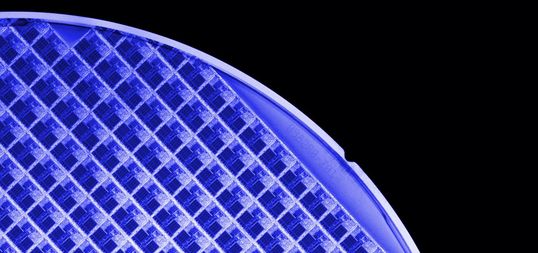
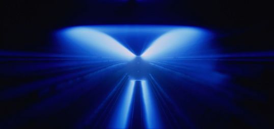
Material removal is used to make electronic component structures from thin layers. Conductor paths or transistors, for example, can then be created. Ionizing the molecules of an assist gas produces ions, which are accelerated in the plasma's electric field towards the substrate surface.

Reactive ion etching enables directional selective ablation, a requirement for the production of microelectronic components and MEMS (micro electro-mechannical systems). To precisely control ion flow and energy, different generators with different excitation frequencies are used to generate bias voltages.

White paper

We have compiled white papers with interesting topics for you

PDF - 715 KB
It depends on the form: bipolar sputtering
Two characteristics of bipolar power supplies are presented in this article: (i) a wide pulse frequency range of up to 100 kHz and (ii) an additional brake time between the positive and negative half-wave of the square wave shape of electricity and voltage.
PDF - 941 KB
Sine or square wave
Since the introduction of dual magnetron sputtering (DMS) for highly insulating layers, it is possible to choose between a square wave pulse and sine wave power supply.
PDF - 567 KB
Auto Frequency Tuning
A countermeasure against rapid fluctuations in the plasma's impedance range is automatic frequency tuning, during which the RF generator sets its fundamental oscillation to a frequency value with better adaptation within a time frame of less than one millisecond.
PDF - 2 MB
New pulsed DC technology
Direct current and pulsed direct current sputtering are some of the most frequently used sputtering techniques in the industrial sector. The introduction of pulsed direct current technology facilitated the mass production of coatings made of non-conductive compounds created by reactive magnetron sputtering.
PDF - 1 MB
Voltage controlled transition mode
Reactive sputtering is a largely successful method used in modern industry to create insulating coatings and hard coatings. In comparison with evaporation, sputtering offers the benefits of the ion-assisted coating, which makes it attractive for the industry despite considerable system and electricity costs.
PDF - 2 MB
Arc management
The creation of arcs during MF magnetron sputtering: A well-known problem during reactive magnetron sputtering is the arc formation at the cathodes.
PDF - 864 KB
LDMOS
This paper explores the effects of performance combining structures on the RF and thermal performance of RF high-power amplifiers under incongruent conditions. 
PDF - 425 KB
HiPIMS - new possibilities for the industry
High Power Impulse Magnetron Sputtering (HIPIMS) is the latest PVD process (Physical Vapor Deposition) available to the industry.
PDF - 1 MB
PEALD technology, radio frequency signal generator and matching networks
Atomic Layer Deposition (ALD) is a process during which a number of thin layer materials are deposited from a vapor phase. A very thin film is built up out of atomic layers in several coating cycles.
PDF - 3 MB
Application of pulsed DC sputtering
One of the most interesting resorption materials for solar cells are copper-indium-selenide (CIS) based materials whose properties can be changed by replacing a part of the indium with gallium to make Cu(In,Ga)Se2, known as CIGS.
PDF - 2 MB
Precision in processing
Continuous improvements to the semiconductor production process are required to ensure a continuous reduction in size. This in turn requires TF generators that have an ever-higher signal quality in relation to output power and time resolution.

Products

Contact
Dr. Jan Peter Engelstädter
Plasma MF
Email
Service & contact