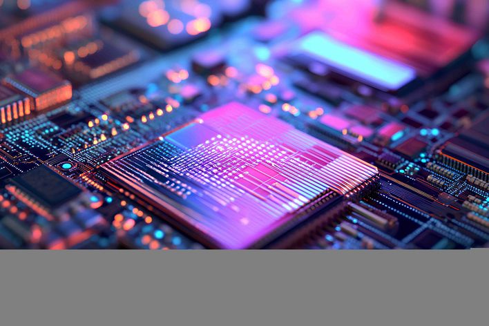
Semi-conductor manufacturing
No AI without TRUMPF. Our laser and plasma solutions are the backbone of modern semi-conductor manufacturing. From EUV lithography to advanced packaging: Our technologies are used wherever the future is being created. Whether coating, exposing or etching – anyone who wants innovation and progress cannot ignore TRUMPF. We think ahead: Our solutions not only enable peak performance, but also resource-saving processes. Together with leading technology partners, we develop innovations that transform entire industries.
Semi-conductors without TRUMPF? Unthinkable.
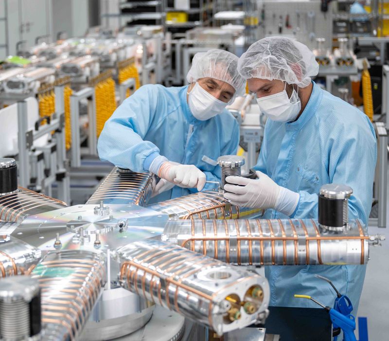
Innovations begin with people. Because behind every advancement lie ideas, passion, and courage. We are helping to produce a new generation of chips. TRUMPF makes semi-conductor manufacturing faster, more sustainable and more efficient. For manufacturers who want to build top-of-the-line chips, TRUMPF is not just a supplier – we are a strategic partner.


How TRUMPF is advancing semi-conductor manufacturing
Our technologies ensure maximum availability in all essential process steps. This takes semi-conductor manufacturing to the next level – faster, more efficient and more sustainable.

1. Ingot slicing
Ultra-thin slices are cut from the silicon crystal. The laser allows chip manufacturers to do this in a particularly material-friendly way.
2. Bare wafers
All the structures of the semi-conductor chips are applied to the bare silicon wafer.
3. Deposition
A thin layer of material, such as insulators or conductors, is placed on the wafer. It is the basis for transistors and connections.
4. Photoresist coating
The wafer is coated with a light-sensitive layer of paint so that specific areas can be selectively exposed and processed.
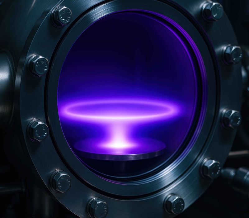
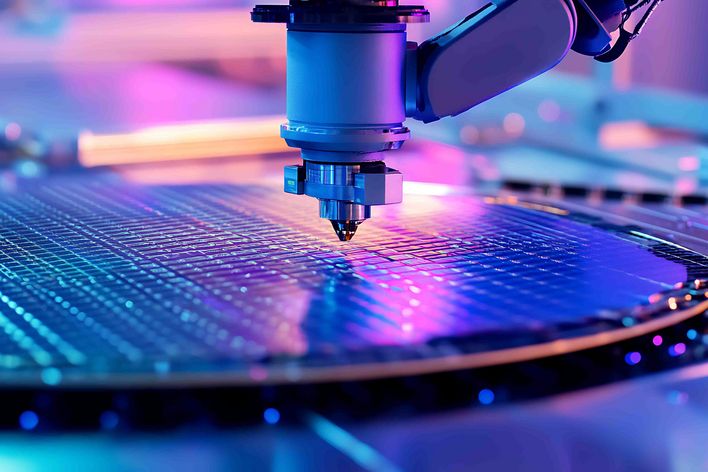
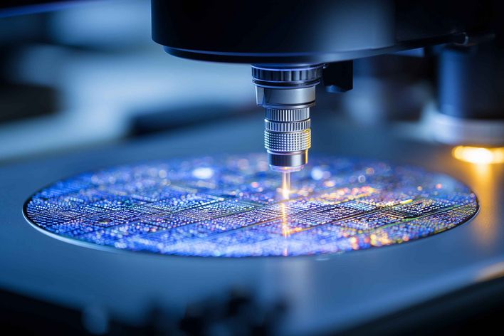
5. EUV lithography
Light is projected onto the paint through a screen, creating tiny structural patterns and thus outlining the subsequent circuits.
6. Etching
The exposed areas are chemically or physically etched away, creating grooves, vias and conductive traces in the material.
7. Ion implant
Foreign atoms are introduced into the silicon at high speed (doping). This changes the electrical properties and the transistors can switch.
8. Chemical Mechanical Polishing (CMP)
The wafer surface is smoothed chemically and mechanically. This enables a multi-layered structure in particularly advanced chips.
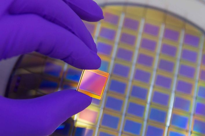
9. Wafer dicing
The wafer is separated into so-called dies. Each die will later become its own microchip. This can be achieved with particular precision using lasers or plasma.
10. Testing
Each chip undergoes electrical testing – first functionally, later also under load and temperature.
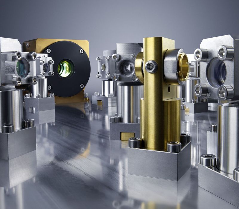
Our products for semi-conductor manufacturing
Our laser and plasma applications are used in all essential production steps of chip manufacturing.
Learn more about the use of the laser now!
Laser technology can make a contribution before, after, and during almost every single production step in chip manufacturing. Every semi-conductor manufacturer and processor has its own process chain in which it can use lasers at different points.
How TRUMPF is shaping the chip industry
How TRUMPF's high-power lasers enable EUV lithography.
Our global partnerships
New generations of chips should consume as little energy as possible. The chips themselves should also be manufactured in the most energy-efficient way possible, and the systems should run around the clock, 365 days a year. TRUMPF fulfills this requirement by supporting all relevant equipment suppliers of chip factories with their manufacturing solutions. As an innovation leader, we deliver electronics and laser solutions for greater efficiency and sustainability in the production of microchips. For many decades, TRUMPF has maintained close partnerships with the leading suppliers of the semi-conductor industry in Asia, the USA and Europe. This trusting and close cooperation enables us to develop innovative solutions that meet the high demands of our customers.
One example of successful collaboration is the long-standing and intensive cooperation with ASML, the world's largest manufacturer of lithography systems. TRUMPF supplies the high-power laser for EUV technology, and thus core technology for the production of the world's most powerful microchips. TRUMPF generators also reliably and precisely supply energy for the coating and etching processes in the production of silicon wafers. TRUMPF's laser technology is used in numerous applications, such as quality control of photomasks and the smallest chip structures.
A world of superlatives
As a high-tech company, we actively shape the future of the semi-conductor industry and make a significant contribution to the digital revolution with our innovations. The next steps include developing even more efficient manufacturing solutions and expanding partnerships to further push the boundaries of technology.

Get inspired! Semicon news, TRUMPF updates, technology insights
Want to find out more?
Then download exciting technical articles and white papers from the world of semi-conductor production here, or feel free to contact us.
Everything you always wanted to know...
A semi-conductor is a material whose conductivity lies between that of a conductor (e.g. copper) and an insulator (e.g. glass). Typical semi-conductor materials are silicon or germanium. Conductivity can be specifically altered by doping (introduction of foreign atoms) and external influences such as temperature or light. This makes semi-conductors ideal for electronic components such as transistors, diodes and integrated circuits. The semi-conductor industry is growing strongly, driven by data warehouses, AI and miniaturization. The trend is towards increasingly powerful yet smaller semi-conductors. Experts call this development the nanometer race. TRUMPF's laser and plasma technologies are essential for processes such as EUV lithography, coating, exposure and etching. Without these technologies, the production of the latest generation of chips would not be possible.
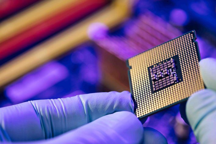
A transistor is an electronic component that serves as a switch or amplifier for electrical signals. It is the heart of modern microelectronics and forms the basis for processors, memory chips and almost all digital devices. More transistors in a chip equate to higher computing power.
A semi-conductor typically goes through several hundred, sometimes over a thousand, production steps. It takes months to manufacture. In a highly simplified way, the semi-conductor manufacturing process can be described in ten steps:
1. The manufacturing process begins with a wafer, which is drawn from high-purity silicon and cut into thin slices.
2. The wafer is polished to create an absolutely smooth surface for the subsequent processes.
3. In lithography, a light-sensitive layer (photoresist) is applied, which later determines the structure of the circuits.
4. Extremely precise exposure methods such as EUV lithography are used to project tiny patterns onto the wafer.
5. The exposed areas are then chemically developed so that the desired structures become visible.
6. Etching processes (e.g. plasma etching) involve removing layers of material to form the conductor tracks and transistors.
7. This is followed by doping processes in which foreign atoms are introduced to change the electrical properties of the silicon.
8. Several layers of metals and insulators are applied to create complex connections between the transistors.
9. After hundreds of such steps, the wafer is tested and cut into individual chips (dies) – this process is called wafer dicing.
10. Finally, the chips are packaged, tested and approved for use in devices such as smartphones, computers or cars.

1. Information and Communication Technology
Semi-conductors control the computing processes in computers, servers, and smartphones. They are indispensable for digital communication, cloud computing and the Internet of Things (IoT).
2. Artificial Intelligence and Data Centers
High-performance chips enable the processing of huge amounts of data for AI applications and big data analytics.
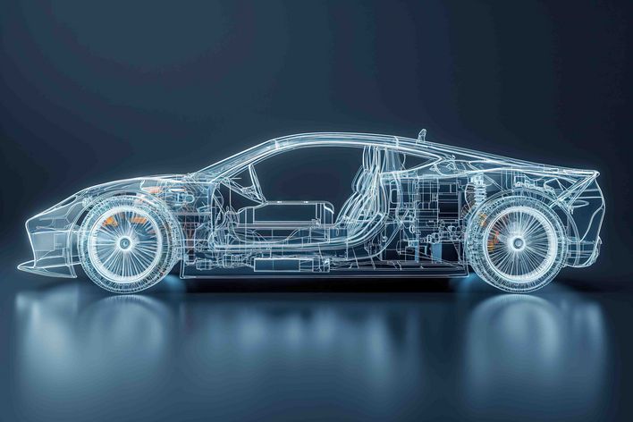
3. Automotive industry
Semi-conductors are essential in vehicles for driver assistance systems, e-mobility, infotainment and autonomous driving.
4. Medical technology
They enable precise imaging, diagnostic systems, and even implantable devices.
5. Industry and Automation
Semi-conductors power sensors, controllers and robotics in industrial manufacturing.

AI applications require enormous computing power. The more powerful the chips, the faster and more efficiently AI models can be trained and deployed. Advances in semi-conductor technology are therefore significantly driving the development of AI. TRUMPF uses technology, such as EUV, to manufacture the most powerful chips.
AI chips are specially designed processors that run complex algorithms for machine learning and artificial intelligence directly on the chip. They differ from classic processors in their ability to process large amounts of data in parallel.
AI chips are created in a highly complex production process that combines classic semi-conductor technologies with innovative packaging methods. First, the actual computing cores, usually based on silicon, are manufactured in nanometer structures.
The chips must be extremely powerful and energy-efficient in order to process huge amounts of data in real time. Therefore, manufacturers are increasingly relying on advanced packaging. In this process, several chips are combined on so-called interposers, which serve as a connecting layer.
While silicon interposers have long been the standard, they are reaching their limits in terms of size and cost. The solution: Glass interposers. Glass is cheaper, can be processed into large panels, and enables complex chip packages for AI systems. To create the electrical connections between the layers, millions of tiny holes, known as Through-Glass Vias (TGVs), must be drilled into the glass. Here too, laser technology from TRUMPF is used.

Moore's Law states that the number of transistors on a microchip doubles approximately every two years, while the cost per computation decreases. This allows the performance of chips to continuously increase without increasing their size. To continue miniaturization, technologies such as EUV lithography and new chip architectures (e.g. 3D structures) are being used. The law was formulated in 1965 by Gordon Moore, co-founder of Intel. It is not a law of nature, but an observation that reflects the speed of innovation in the industry.

1. Miniaturization and precision
The industry is under enormous pressure to produce ever smaller structures in the nanometer range. EUV lithography and plasma generators must operate with extreme precision to create 3D structures on silicon wafers. Even the smallest deviations lead to rejects and high costs. Quality control (metrology) is becoming increasingly complex, as tolerances are in the nanometer range.
2. Power input and sustainability
Energy efficiency is crucial for reducing operating costs and achieving sustainability goals. Plasma generators and laser systems must therefore operate as energy-efficiently as possible.
3. Supply chains and quality assurance
The entire supply chain must ensure zero-error quality. Weaknesses on behalf of suppliers can jeopardize production. TRUMPF demands strict quality standards from its partners and suppliers.
4. Availability of production systems
Semi-conductor production is heavily concentrated in Asia. The equipment suppliers must deliver the highest service quality to n chip manufacturers worldwide to avoid downtimes. TRUMPF is therefore investing in regional service hubs and technology centers, for example in Taiwan.

Lithography is a key process in semi-conductor manufacturing, in which structures for electronic circuits are transferred onto silicon wafers. In this process, a special coating device applies a light-sensitive layer (photoresist) to the wafer. The lithography system then exposes the desired patterns using light and develops them chemically. These structures form the basis for transistors and other components on the chip. The most advanced technology in this field is EUV lithography. It uses extremely short-wavelength light to create nanometer-sized structures. The most powerful microchips cannot be manufactured without EUV lithography. It is crucial for the implementation of Moore's Law, which predicts a doubling of the number of transistors every two years.
A wafer is the starting point for the production of microchips. It consists of high-purity silicon, which is first grown into a single crystal and then cut into thin slices. These discs are polished to create an absolutely smooth surface. The structures of the circuits are created on the wafer through lithography, laser exposure, etching processes and doping. After hundreds of process steps, the wafer is tested and cut into individual chips (“dies”).
Wafer dicing refers to the process of separating semi-conductor chips from a wafer. This is a key step in the backend of the semi-conductor process chain.
Mechanical sawing, stealth dicing, ablative laser dicing and plasma dicing.

Plasma etching is a process in which material is removed or structured from the wafer surface using ionized gas (plasma). This process is essential for a precise chip structure.

A device that supplies high-frequency electrical energy to generate and control plasma for chip manufacturing.

Through-glass vias (TGVs) are tiny, conductive vias in glass that enable electrical connections between different layers of a chip package. They are crucial for high-performance applications because they shorten signal paths and minimize energy losses.

Semi-conductor production requires a lot of energy. Semi-conductor companies can significantly reduce their CO₂ footprint by relying on energy-efficient technologies and circular economy; TRUMPF technology plays a key role here. Sustainability is part of TRUMPF's DNA as a family business. Therefore, with forward-looking technologies such as EUV lithography, we place the utmost importance on using energy and materials efficiently and sparingly.