More than three times faster than conventional sawing methods // High cut edge quality similar to plasma dicing // High-speed laser dicing makes semiconductor production more efficient
Semicon Korea trade fair: LIDROTEC and TRUMPF accelerate wafer dicing in the chip industry
Ditzingen/Bochum/Seoul, February 9 2026 – High-tech company LIDROTEC has developed an innovative laser dicing process. TRUMPF has helped to scale the process for mass production of wafers with its laser and beam shaping technology. This enables users to cut wafers more than three times faster than with conventional sawing processes, while maintaining high cut edge quality. “The new laser dicing process goes beyond the limits of established methods. It enables the chip industry to manufacture the next generation of semiconductors faster, more economically, and in high quality,” says Christian Weddeling, responsible for wafer dicing at TRUMPF. TRUMPF and LIDROTEC are presenting the new technology at the Semicon Korea trade fair in Seoul.
Three times faster than mechanical saws
Separating semiconductor chips from a wafer is an important step in the backend of semiconductor manufacturing. The new process from LIDROTEC combines ablative laser dicing under a liquid stream with high-precision beam shaping technology from TRUMPF. Users benefit from a significant increase in productivity, as the cutting speeds are more than three times faster than those of mechanical saws. At the same time, the technology provides the highest cutting edge quality, which is equivalent to plasma dicing. The liquid immediately removes molten and solidified material residues. This reduces post-processing and increases the yield of defect-free chips.
Less maintenance and lower operating costs
Since users do not need mechanical wear parts such as saw blades, both maintenance and operating costs are reduced compared to the sawing process. " The combination of speed, high yield of defect-free parts, and reduced material consumption helps our technology make semiconductor production more efficient and economical," says Alexander Kanitz, CTO of LIDROTEC. In addition, the process can be flexibly adapted to different materials such as silicon, silicon carbide, or hybrid wafer structures, making it suitable for a wide range of semiconductor types.
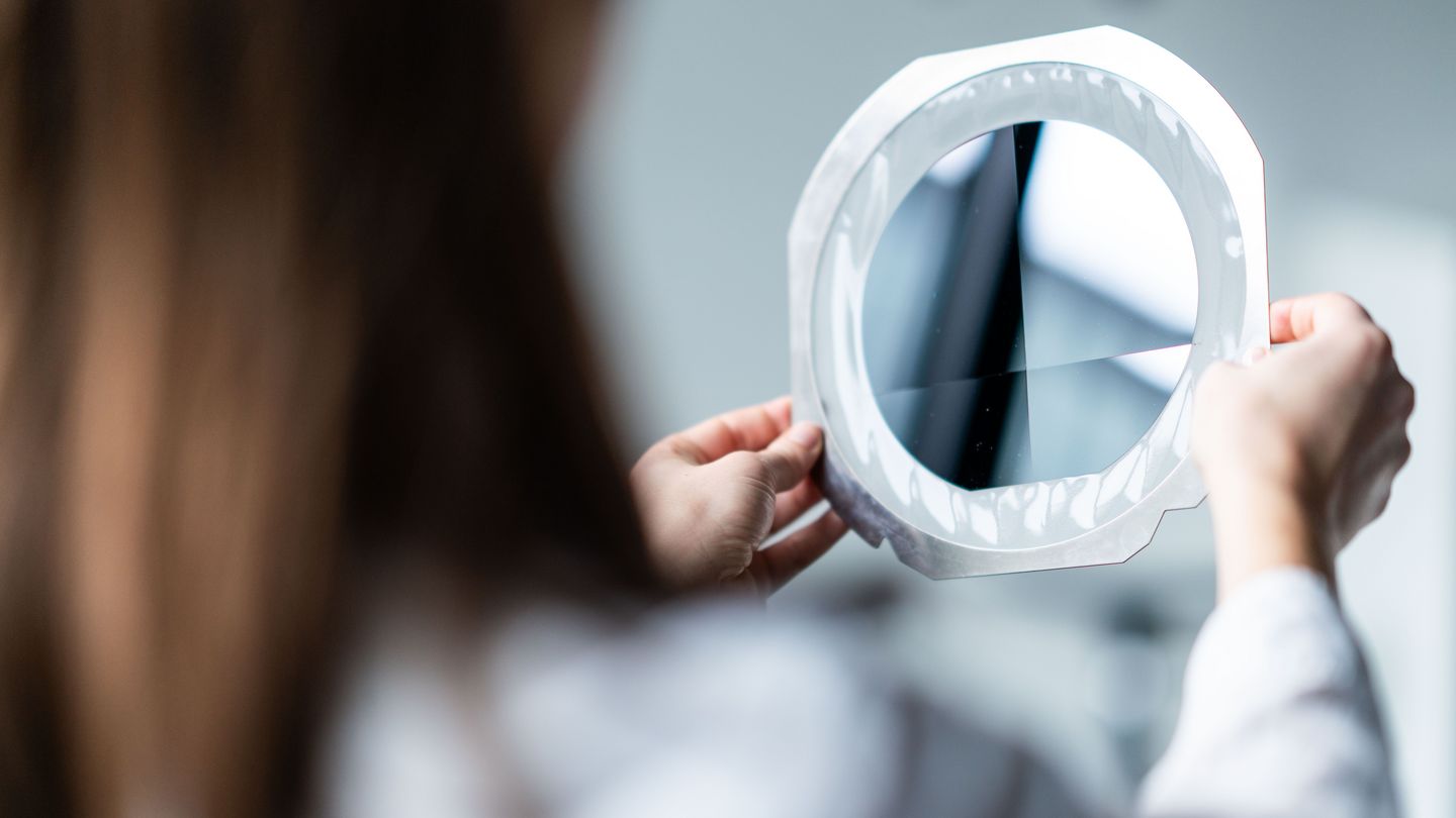
Wafer dicing
The new laser-assisted process makes wafer cutting significantly more productive.
Image source: TRUMPF
K této tiskové informaci jsou připraveny vhodné digitální obrazy v rozlišení vhodném pro tisk. Ty smějí být používány pouze k redakčním účelům. Používání je bez honoráře při uvedení zdroje „Foto: TRUMPF“. Grafické změny – kromě k uvolnění hlavního motivu – nejsou povoleny. Další fotografie lze vyvolat v TRUMPF Media Pool.

The new laser-assisted process makes wafer cutting significantly more productive.
Image source: TRUMPF


Ansprechpartner